
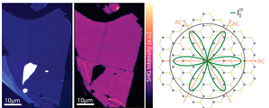
Peeling graphite layer by layer reveals the charge exchange dynamics of ions inside a solid
A. Niggas, S. Creutzburg, J. Schwestka, B. Wöckinger, T. Gupta, P. L. Grande, D. Eder, J. P. Marques, B. C. Bayer, F. Aumayr, R. Bennett, and R. A. Wilhelm
Communications Physics 4, 180 (2021)
Press release: https://www.tuwien.at/en/tu-wien/news/news-articles/news/wie-sich-ionen-ihre-elektronen-zurueckholen
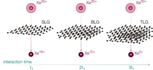
Over seventy years ago, Niels Bohr described how the charge state of an atomic ion moving through a solid changes dynamically as a result of electron capture and loss processes, eventually resulting in an equilibrium charge state. Although obvious, this process has so far eluded direct experimental observation. By peeling a solid, such as graphite, layer by layer, and studying the transmission of highly charged ions through single-, bi- and trilayer graphene, we can now observe dynamical changes in ion charge states with monolayer precision. In addition we present a first-principles approach based on the virtual photon model for interparticle energy transfer to corroborate our findings. Our model that uses a Gaussian shaped dynamic polarisability rather than a spatial delta function is a major step in providing a self-consistent description for interparticle de-excitation processes at the limit of small separations.
https://www.nature.com/articles/s42005-021-00686-1
Phonon renormalization in reconstructed MoS2 moiré superlattices
J. Quan, L. Linhart, M.-L. Lin, D. Lee, J Zhu, C.-Y. Wang, W.-T. Hsu, J. Choi, J. Embley, C. Young, T. Taniguchi, K. Watanabe, C.-K. Shih, K Lai, A. H. MacDonald, P.-H. Tan, F. Libisch, and X. Li
Nature Materials, 10.1038/s41563-021-00960-1 (2021)
Press Release here: https://www.tuwien.at/tu-wien/aktuelles/news/news/moire-effekt-wie-man-materialeigenschaften-verdrehen-kann
In moiré crystals formed by stacking van der Waals materials, surprisingly diverse correlated electronic phases and optical properties can be realized by a subtle change in the twist angle. Here, we discover that phonon spectra are also renormalized in MoS2 twisted bilayers, adding an insight to moiré physics. Over a range of small twist angles, the phonon spectra evolve rapidly owing to ultra-strong coupling between different phonon modes and atomic reconstructions of the moiré pattern. We develop a low-energy continuum model for phonons that overcomes the outstanding challenge of calculating the properties of large moiré supercells and successfully captures the essential experimental observations. Remarkably, simple optical spectroscopy experiments can provide information on strain and lattice distortions in moiré crystals with nanometre-size supercells. The model promotes a comprehensive and unified understanding of the structural, optical and electronic properties of moiré superlattices.
https://www.nature.com/articles/s41563-021-00960-1
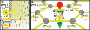
Atomic-Scale Carving of Nanopores into a van der Waals Heterostructure with Slow Highly Charged Ions
J. Schwestka, H. Inani, M. Tripathi, A. Niggas, N. McEvoy, F. Libisch, F. Aumayr, J. Kotakoski, and R. A. Wilhelm
ACS Nano, 10.1021/acsnano.0c04476 (2020)
Press Release here: https://www.tuwien.at/en/tu-wien/news/news-articles/news/the-art-of-making-tiny-holes/
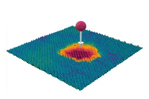
The growing family of 2D materials led not long ago to combining different 2D layers and building artificial systems in the form of van-der-Waals heterostructures. Tailoring of heterostructure properties post-growth would greatly benefit from a modification technique with a monolayer precision. However, appropriate techniques for material modification with this precision are still missing. To achieve such control, slow highly charged ions appear ideal as they carry high amounts of potential energy, which is released rapidly upon ion neutralization at the position of the ion. The resulting potential energy deposition is thus limited to just a few atomic layers (in contrast to the kinetic energy deposition). Here, we irradiated a freestanding van-der-Waals MoS2/graphene heterostructure with 1.3 keV/amu xenon ions in high charge states of 38, which led to nm-sized pores that appear only in the MoS2 facing the ion beam, but not in graphene beneath the hole. Reversing the stacking order leaves both layers undamaged, which we attribute to the high conductivity and carrier mobility in graphene acting as a shield for the MoS2 underneath. Our main focus is here on monolayer MoS2, but we also analyzed areas with few-layer structures, and observed that the perforation is limited to the two topmost MoS2 layers, whereas deeper layers remain intact. Our results demonstrate that in addition to already being a valuable tool for materials processing, the usability of ion irradiation can be extended to mono(or bi-)layer manipulation of van-der-Waals heterostructures when also the localized potential energy deposition of highly charged ions is added to the toolbox.
https://pubs.acs.org/doi/10.1021/acsnano.0c04476
Vanishing influence of the band gap on the charge exchange of slow highly charged ions in freestanding single-layer MoS2
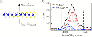
Charge exchange and kinetic energy loss of slow highly charged xenon ions transmitted through freestanding monolayer MoS2 are studied. Two distinct exit charge state distributions, characterized by high and low charge states, are observed. They are accompanied by smaller and larger kinetic energy losses, as well as scattering angles, respectively. High charge exchange is attributed to two-center neutralization processes, which take place in close impact collisions with the target atoms. Experimental findings are compared to graphene as a target material and simulations based on a time-dependent scattering potential model. Independent of the target material, experimentally observed charge exchange can be modeled by the same electron capture and de-excitation rates for MoS2 and graphene. A common dependence of the kinetic energy loss on the charge exchange for MoS2 as well as graphene is also observed. Considering the similarities of the zero band-gap material graphene and the 1.9 eV band-gap material MoS2, we suggest that electron transport on the femtosecond timescale is dominated by the strong influence of the ion's Coulomb potential in contrast to the dispersion defined by the material's band structure.
journals.aps.org/prb/abstract/10.1103/PhysRevB.102.045408
Phys. Rev. B 102, 045408 (2020)
The role of contaminations in ion beam spectroscopy with freestanding 2D materials: A study on thermal treatment
A. Niggas, J. Schwestka, S. Creutzburg, T. Gupta, D. Eder, B. C. Bayer, F. Aumayr, and R. A. Wilhelm
J. Chem. Phys. 153, 014702 (2020)
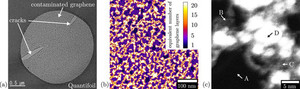
As surface-only materials, freestanding 2D materials are known to have a high level of contamination—mostly in the form of hydrocarbons, water, and residuals from production and exfoliation. For well-designed experiments, it is of particular importance to develop effective cleaning procedures, especially since standard surface science techniques are typically not applicable. We perform ion spectroscopy with highly charged ions transmitted through freestanding atomically thin materials and present two techniques to achieve clean samples, both based on thermal treatment. Ion charge exchange and energy loss are used to analyze the degree of sample contamination. We find that even after cleaning, heavily contaminated spots remain on single layer graphene. The contamination coverage, however, clusters in strand-like structures leaving large clean areas. We present a way to discriminate clean from contaminated areas with our ion beam spectroscopy if the heterogeneity of the surface is increased sufficiently enough. We expect a similar discrimination to be necessary in most other experimental techniques.
https://doi.org/10.1063/5.0011255
Energy landscapes of graphene under general deformations: DFT-to-hyperelasticity upscaling
R. Höller, V. Smejkal, F. Libisch, and C. Hellmich
International Journal of Engineering Science 154, 103342 (2020)
Profound investigation of the unsurpassed mechanical properties of suspended graphene motivates the link between classical continuum mechanics (where the notions of “mechanical strength”, “mechanical stiffness”, and “elastic energy” have actually been coined) and density functional theory (DFT) rooted in quantum mechanics. Namely, the latter quantifies the energetic ground states of systems consisting of atomic nuclei and electrons; and these ground states, in turn, are directly linked to the elastic energy. While the corresponding state-of-the-art typically concerns graphene mechanics under uniaxial or equally biaxial strain states, we here present a fully anisotropic free (strain) energy function reflecting DFT-simulations associated with tens of thousands of arbitrary biaxial strain states. The latter are realized as sets of primitive unit cell vectors spanning a rhomboid unit cell hosting two carbon atoms. The position of the latter follows from internal energy minimization through the Vienna ab initio simulation package (VASP). As corresponding continuum mechanical representation we employ hyperelastic, structure tensor-based polynomial models up to the fifth order. The corresponding stress-strain relations are of concave nature, and hence, they provide access to the failure limits of the 2D material undergoing arbitrary loading situations. This is expected to introduce a new level of precision in the growing field of the structural mechanics of graphene.
https://www.sciencedirect.com/science/article/pii/S0020722520301300
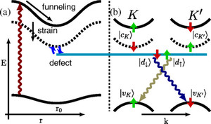
Band Nesting in Two-Dimensional Crystals: An Exceptionally Sensitive Probe of Strain
L. Mennel, V. Smejkal, L. Linhart, J. Burgdörfer, F. Libisch, and T. Mueller
Nano Letters, doi 10.1021/acs.nanolett.0c00694 (2020)
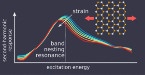
Band nesting occurs when conduction and valence bands are approximately equispaced over regions in the Brillouin zone. In two-dimensional materials, band nesting results in singularities of the joint density of states and thus in a strongly enhanced optical response at resonant frequencies. We exploit the high sensitivity of such resonances to small changes in the band structure to sensitively probe strain in semiconducting transition metal dichalcogenides (TMDs). We measure and calculate the polarization-resolved optical second harmonic generation (SHG) at the band nesting energies and present the first measurements of the energy-dependent nonlinear photoelastic effect in atomically thin TMDs (MoS2, MoSe2, WS2, and WSe2) combined with a theoretical analysis of the underlying processes. Experiment and theory are found to be in good qualitative agreement displaying a strong energy dependence of the SHG, which can be exploited to achieve exceptionally strong modulation of the SHG under strain. We attribute this sensitivity to a redistribution of the joint density of states for the optical response in the band nesting region. We predict that this exceptional strain sensitivity is a general property of all 2D materials with band nesting.
http://dx.doi.org/10.1021/acs.nanolett.0c00694
Growth of In2O3(111) thin films with optimized surfaces
Phys. Rev. Materials 3, 103403 (2019)
Indium oxide is widely employed in applications ranging from optoelectronics and gas sensing to catalysis, as well as in thin-film heterostructures. To probe the fundamentals of phenomena at the heart of In2O3-based devices that are tied to the intrinsic surface and interface properties of the material, well-defined single-crystalline In2O3 surfaces are needed. We report on how to grow atomically flat In2O3(111) thin films on yttria-stabilized zirconia substrates by pulsed laser deposition. The films are largely relaxed and reproduce the atomic-scale details of the surfaces of single crystals, except for line defects originating from the antiphase domain boundaries that form because of the one-on-four lattice match between the surface unit cells of In2O3(111) and of the substrate. While optimizing the growth conditions, we observe that the morphology of the films is ruled by the oxygen chemical potential, which determines the nature and diffusivity of adspecies during growth.
doi.org/10.1103/PhysRevMaterials.3.103403
Localized Intervalley Defect Excitons as Single-Photon Emitters in WSe2
Phys. Rev. Lett. 123, 146401 (2019)
Single-photon emitters play a key role in present and emerging quantum technologies. Several recent measurements have established monolayer WSe2 as a promising candidate for a reliable single-photon source. The origin and underlying microscopic processes have remained, however, largely elusive. We present a multiscale tight-binding simulation for the optical spectra of WSe2 under nonuniform strain and in the presence of point defects employing the Bethe-Salpeter equation. Strain locally shifts excitonic energy levels into the band gap where they overlap with localized intragap defect states. The resulting hybridization allows for efficient filling and subsequent radiative decay of the defect states. We identify intervalley defect excitonic states as the likely candidate for antibunched single-photon emission. This proposed scenario is shown to account for a large variety of experimental observations including brightness, radiative transition rates, the variation of the excitonic energy with applied magnetic and electric fields as well as the variation of the polarization of the emitted photon with the magnetic field.
https://doi.org/10.1103/PhysRevLett.123.146401
Charge-Exchange-Driven Low-Energy Electron Splash Induced by Heavy Ion Impact on Condensed Matter
J. Schwestka, A. Niggas, S. Creutzburg, R. Kozubek, R. Heller, M. Schleberger, R. A. Wilhelm, and F. Aumayr*
J. Phys. Chem. Lett.201910XXX4805-4811(2019)
See also this Press Release (in german) https://www.tuwien.at/tu-wien/aktuelles/news/news/langsame-elektronen-gegen-den-krebs/ !
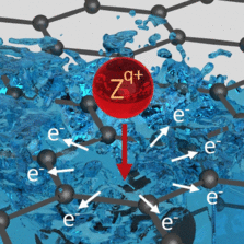
Low-energy electrons (LEEs) are of great relevance for ion-induced radiation damage in cells and genes. We show that charge exchange of ions leads to LEE emission upon impact on condensed matter. By using a graphene monolayer as a simple model system for condensed organic matter and utilizing slow highly charged ions (HCIs) as projectiles, we highlight the importance of charge exchange alone for LEE emission. We find a large number of ejected electrons resulting from individual ion impacts (up to 80 electrons/ion for Xe40+). More than 90% of emitted electrons have energies well below 15 eV. This “splash” of low-energy electrons is interpreted as the consequence of ion deexcitation via an interatomic Coulombic decay (ICD) process.
doi.org/10.1021/acs.jpclett.9b01774
Ultrathin calcium fluoride insulators for two-dimensional field-effect transistors
Y. Illarionov, A. Banshchikov, D. Polyushkin, S. Wachter, T. Knobloch, M. Thesberg, L. Mennel, M. Paur, M. Stöger-Pollach, A. Steiger-Thirsfeld, M. Vexler, M. Waltl, N. Sokolov, T. Mueller, and T. Grasser
Nature Electronics 10.1038/s41928-019-0256-8 (2019)
See also this press release: https://www.tuwien.at/en/tu-wien/news/news-articles/news/ultrathin-transistors-for-faster-computer-chips/
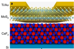
Two-dimensional semiconductors could be used to fabricate ultimately scaled field-effect transistors and more-than-Moore nanoelectronic devices. However, these targets cannot be reached without appropriate gate insulators that are scalable to the nanometre range. Typically used oxides such as SiO2, Al2O3 and HfO2 are, however, amorphous when scaled, and 2D hexagonal boron nitride exhibits excessive gate leakage currents. Here, we show that epitaxial calcium fluoride (CaF2), which can form a quasi van der Waals interface with 2D semiconductors, can serve as an ultrathin gate insulator for 2D devices. We fabricate scalable bilayer MoS2 field-effect transistors with a crystalline CaF2 insulator of ~2 nm thickness, which corresponds to an equivalent oxide thickness of less than 1 nm. Our devices exhibit low leakage currents and competitive device performance characteristics, including subthreshold swings down to 90 mV dec−1, on/off current ratios up to 107 and a small hysteresis.
www.nature.com/articles/s41928-019-0256-8
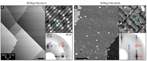
Pushing the detection of cation nonstoichiometry to the limit
Phys. Rev. Materials 3, 043802, (2019)
Nanoscale complex-oxide thin films prepared by well-established growth techniques, such as pulsed-laser deposition or molecular-beam epitaxy, often exhibit compositions that deviate from the ideal stoichiometry. Even small variations in composition can lead to substantial changes in the technologically relevant electronic, magnetic, and optical properties of these materials. To assess the reasons behind this variability, and ultimately to allow tuning the properties of oxide films with precise control of the deposition parameters, high-resolution detection of the nonstoichiometry introduced during growth is needed. The resolution of current techniques, such as x-ray diffraction, fluorescence, or spectroscopy, is limited to estimating composition differences in the percent level, which is often insufficient for electronic-device quality. We develop an unconventional approach based on scanning tunneling microscopy for enabling the determination of cation imbalance introduced in thin films with exceptionally small detection limit. We take advantage of the well-controlled surface reconstructions on SrTiO3(110), and use the established relation between those reconstructions and the surface composition to assess the cation excess deposited in pulsed-laser grown SrTiO3(110) films. We demonstrate that a <0.1% change in cation nonstoichiometry is detectable by our approach. Furthermore, we show that, for thin films that accommodate all the nonstoichiometry at the surface, this method has no fundamental detection limit.
https://journals.aps.org/prmaterials/abstract/10.1103/PhysRevMaterials.3.043802
Second harmonic generation in strained transition metal dichalcogenide monolayers: MoS2, MoSe2, WS2, and WSe2
L. Mennel, M. Paur, and T. Mueller
APL Photonics 4, 034404 (2019)
https://doi.org/10.1063/1.5051965
Electroluminescence from multi-particle exciton complexes in transition metal dichalcogenide semiconductors
M. Paur, A. J. Molina-Mendoza, R. Bratschitsch, K. Watanabe, T. Taniguchi, and T. Mueller
Nature Communications 10, 1709 (2019)
Light emission from higher-order correlated excitonic states has been recently reported in hBN-encapsulated monolayer WSe2 and WS2 upon optical excitation. These exciton complexes are found to be bound states of excitons residing in opposite valleys in momentum space, a promising feature that could be employed in valleytronics or other novel optoelectronic devices. However, electrically-driven light emission from such exciton species is still lacking. Here we report electroluminescence from bright and dark excitons, negatively charged trions and neutral and negatively charged biexcitons, generated by a pulsed gate voltage, in hexagonal boron nitride encapsulated monolayer WSe2 and WS2 with graphene as electrode. By tailoring the pulse parameters we are able to tune the emission intensity of the different exciton species in both materials. We find the electroluminescence from charged biexcitons and dark excitons to be as narrow as 2.8 meV.
www.nature.com/articles/s41467-019-09781-y
Atomic-Scale Structure of the Hematite α-Fe2O3(11̅02) “R-Cut” Surface
F. Kraushofer, Z. Jakub, M. Bichler, J. Hulva, P. Drmota, M. Weinold, M. Schmid, M. Setvin, U. Diebold, and G. S. Parkinson
J. Phys. Chem. C 122, 1657 (2018)
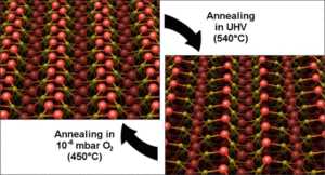
The α-Fe2O3(11̅02) surface (also known as the hematite r-cut or (012) surface) was studied using low-energy electron diffraction (LEED), X-ray photoelectron spectroscopy (XPS), ultraviolet photoelectron spectroscopy (UPS), scanning tunneling microscopy (STM), noncontact atomic force microscopy (nc-AFM), and ab initio density functional theory (DFT)+U calculations. Two surface structures are stable under ultrahigh vacuum (UHV) conditions; a stoichiometric (1 × 1) surface can be prepared by annealing at 450 °C in ≈10–6 mbar O2, and a reduced (2 × 1) reconstruction is formed by UHV annealing at 540 °C. The (1 × 1) surface is close to an ideal bulk termination, and the undercoordinated surface Fe atoms reduce the surface bandgap by ≈0.2 eV with respect to the bulk. The work function is measured to be 5.7 ± 0.2 eV, and the VBM is located 1.5 ± 0.1 eV below EF. The images obtained from the (2 × 1) reconstruction cannot be reconciled with previously proposed models, and a new “alternating trench” structure is proposed based on an ordered removal of lattice oxygen atoms. DFT+U calculations show that this surface is favored in reducing conditions and that 4-fold-coordinated Fe2+ cations at the surface introduce gap states approximately 1 eV below EF. The work function on the (2 × 1) termination is 5.4 ± 0.2 eV.
https://dx.doi.org/10.1021/acs.jpcc.7b10515
Neutralization Dynamics of Slow Highly Charged Ions in 2D Materials
R. Wilhelm, E. Gruber, J. Schwestka, R. Heller, S. Fascko, and F. Aumayr
Applied Sciences 8, 1050 (2018)
We review experimental and theoretical work on the interaction of slow highly charged ions with two-dimensional materials. Earlier work in the field is summarized and more recent studies on 1 nm thick amorphous carbon nanomembranes and freestanding single layer graphene by the authors are reviewed. To explain the findings, models for energy loss determination as well as qualitative model descriptions for the observed ultrafast neutralization dynamics are discussed. The results shown in this paper will be put into context with findings of nanostructure formation on two-dimensional materials, both freestanding and on substrate, as well as on surfaces of bulk insulators.
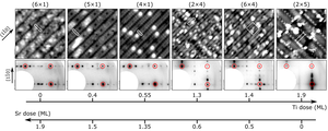
Influence of surface atomic structure demonstrated on oxygen incorporation mechanism at a model perovskite oxide
Nature Communication 9, 3710 (2018)
Michele Riva, Markus Kubicek, Xianfeng Hao, Giada Franceschi, Stefan Gerhold, Michael Schmid, Herbert Hutter, Juergen Fleig, Cesare Franchini, Bilge Yildiz and Ulrike Diebold
Perovskite oxide surfaces catalyze oxygen exchange reactions that are crucial for fuel cells, electrolyzers, and thermochemical fuel synthesis. Here, by bridging the gap between surface analysis with atomic resolution and oxygen exchange kinetics measurements, we demonstrate how the exact surface atomic structure can determine the reactivity for oxygen exchange reactions on a model perovskite oxide. Two precisely controlled surface reconstructions with (4 × 1) and (2 × 5) symmetry on 0.5 wt.% Nb-doped SrTiO3(110) were subjected to isotopically labeled oxygen exchange at 450 °C. The oxygen incorporation rate is three times higher on the (4 × 1) surface phase compared to the (2 × 5). Common models of surface reactivity based on the availability of oxygen vacancies or on the ease of electron transfer cannot account for this difference. We propose a structure-driven oxygen exchange mechanism, relying on the flexibility of the surface coordination polyhedra that transform upon dissociation of oxygen molecules.
Optical imaging of strain in two-dimensional crystals
Nature Communications 9, 516 (2018)
Lukas Mennel, Marco M. Furchi, Stefan Wachter, Matthias Paur, Dmitry K. Polyushkin and Thomas Mueller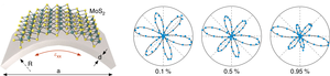
Strain engineering is widely used in material science to tune the (opto-)electronic properties of materials and enhance the performance of devices. Two-dimensional atomic crystals are a versatile playground to study the influence of strain, as they can sustain very large deformations without breaking. Various optical techniques have been employed to probe strain in two-dimensional materials, including micro-Raman and photoluminescence spectroscopy. Here we demonstrate that optical second harmonic generation constitutes an even more powerful technique, as it allows extraction of the full strain tensor with a spatial resolution below the optical diffraction limit. Our method is based on the strain-induced modification of the nonlinear susceptibility tensor due to a photoelastic effect. Using a two-point bending technique, we determine the photoelastic tensor elements of molybdenum disulfide. Once identified, these parameters allow us to spatially image the two-dimensional strain field in an inhomogeneously strained sample.
https://doi.org/10.1038/s41467-018-02830-y
A versatile ion beam spectrometer for studies of ion interaction with 2D materials
Review of Scientific Instruments 89 (2018) 085101 (8 pages)
J. Schwestka, D. Melinc, R. Heller, A. Niggas, L. Leonhartsberger, H. Winter, S. Facsko, F. Aumayr, and R. A. Wilhelm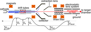
We present an ultrahigh vacuum setup for ion spectroscopy of freestanding two-dimensional solid targets. An ion beam of different ion species (e.g., Xe with charge states from 1 to 44 and Ar with charge states from 1 to 18) and kinetic energies ranging from a few 10 eV to 400 keV is produced in an electron beam ion source. Ions are detected after their transmission through the 2D target with a position sensitive microchannel plate detector allowing the determination of the ion’s exit charge state as well as the scattering angle with a resolution of approximately 0.04 . Furthermore, the spectrometer is mounted on a swiveling frame covering a scattering angle of ±8 with respect to the incoming beam direction. By utilizing a beam chopper, we measure the time-of-flight of the projectiles and determine the energy loss when passing a 2D target with an energy uncertainty of about 2%. Additional detectors are mounted close to the target to observe emitted secondary particles and are read-out in coincidence with the position and time information of the ion detector. A signal in these detectors can also be used as a start trigger for time-of-flight measurements, which then yield an energy resolution of 1% and an approximately 1000-fold larger duty cycle. First results on the interaction of slow Xe 30+ ions with a freestanding single layer of graphene obtained with the new setup are compared to recently published data where charge exchange and energy were measured by means of an electrostatic analyzer. Published by AIP Publishing.
https://doi.org/10.1063/1.5037798
Adsorption of CO on the Fe3O4 surface
J. Phys. Chem. B 122 (2018) 721 (9 pages)
Jan Hulva, Zdenek Jakub, Zbynek Novotny, Niclas Johansson, Jan Knudsen, Joachim Schnadt, Michael Schmid, Ulrike Diebold, and Gareth S. Parkinson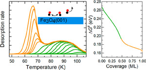
The interaction of CO with the Fe3O4(001)-(√2 × √2)R45° surface was studied using temperature-programmed desorption (TPD), scanning tunneling microscopy (STM), and X-ray photoelectron spectroscopy (XPS), the latter both under ultrahigh vacuum (UHV) conditions and in CO pressures up to 1 mbar. In general, the CO–Fe3O4 interaction is found to be weak. The strongest adsorption occurs at surface defects, leading to small TPD peaks at 115, 130, and 190 K. Desorption from the regular surface occurs in two distinct regimes. For coverages up to two CO molecules per (√2 × √2)R45° unit cell, the desorption maximum shows a large shift with increasing coverage, from initially 105 to 70 K. For coverages between 2 and 4 molecules per (√2 × √2)R45° unit cell, a much sharper desorption feature emerges at ∼65 K. Thermodynamic analysis of the TPD data suggests a phase transition from a dilute 2D gas into an ordered overlayer with CO molecules bound to surface Fe3+ sites. XPS data acquired at 45 K in UHV are consistent with physisorption. Some carbon-containing species are observed in the near-ambient-pressure XPS experiments at room temperature but are attributed to contamination and/or reaction with CO with water from the residual gas. No evidence was found for surface reduction or carburization by CO molecules.
http://pubs.acs.org/doi/full/10.1021/acs.jpcb.7b06349
The role of radiative de-excitation in the neutralization process of highly charged ions interacting with a single layer of graphene
Nucl. Instr. Meth B 422 (2018) 63 (5 pages)
J. Schwestka, R.A. Wilhelm, E. Gruber, R. Heller, R. Kozubek, M. Schleberger, S.Facsko, and F. Aumayr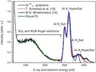
X-ray emission of slow (<1 a.u.) highly charged Argon and Xenon ions is measured for transmission through a freestanding single layer of graphene. To discriminate against X-ray emission originating from the graphene's support grid a coincidence technique is used. X-ray emission of 75 keV Ar17+ and Ar18+ ions with either one or two K-shell vacancies is recorded. Using a windowless Bruker XFlash detector allows us to measure additionally Ar KLL and KLM Auger electrons and determine the branching ratio of radiative vs. non-radiative decay of Ar K-shell holes. Furthermore, X-ray spectra for 100 keV Xe22+-Xe35+ ions are compared, showing a broad M-line peak for all cases, where M-shell vacancies are present. All these peaks are accompanied by emission lines at still higher energies indicating the presence of a hollow atom during X-ray decay. We report a linear shift of the main M-line peak to higher energies for increasing incident charge state, i.e. increasing number of M-shell holes.
https://doi.org/10.1016/j.nimb.2018.02.022
Accurate modeling of defects in graphene transport calculations
Phys. Rev. B 97 , 035430 (2018)
L. Linhart, J. Burgdörfer, and F. Libisch
We present an approach for embedding defect structures modeled by density functional theory into large-scale tight-binding simulations. We extract local tight-binding parameters for the vicinity of the defect site using Wannier functions. In the transition region between the bulk lattice and the defect the tight-binding parameters are continuously adjusted to approach the bulk limit far away from the defect. This embedding approach allows for an accurate high-level treatment of the defect orbitals using as many as ten nearest neighbors while keeping a small number of nearest neighbors in the bulk to render the overall computational cost reasonable. As an example of our approach, we consider an extended graphene lattice decorated with Stone-Wales defects, flower defects, double vacancies, or silicon substitutes. We predict distinct scattering patterns mirroring the defect symmetries and magnitude that should be experimentally accessible.
https://doi.org/10.1103/PhysRevB.97.035430
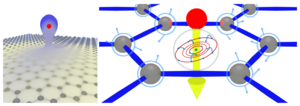
Interatomic Coulombic Decay - the mechanism for rapid de-excitation of hollow atoms
Physical Review Letters 119 (2017) 13401 (6 pages)
R.A. Wilhelm, E. Gruber, J. Schwestka, R. Kozubek, T.I. Madeira, J.P. Marques, J. Kobus, A.V. Krasheninnikov, M. Schleberger, and F. Aumayr
The impact of a highly charged ion onto a solid gives rise to charge exchange between the ion and target atoms, so that a slow ion gets neutralized in the vicinity of the surface. Using highly charged Ar and Xe ions and the surface-only material graphene as a target, we show that the neutralization and deexcitation of the ions proceeds on a sub-10 fs time scale. We further demonstrate that a multiple Interatomic Coulombic Decay (ICD) model can describe the observed ultrafast deexcitation. Other deexcitation mechanisms involving nonradiative decay and quasimolecular orbital formation during the impact are not important, as follows from the comparison of our experimental data with the results of first-principles calculations. Our method also enables the estimation of ICD rates directly.